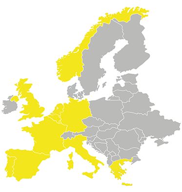
Background of the Chips Joint Undertaking
The Chips Joint Undertaking (JU) is a collaborative initiative between the public and private sectors, aimed at enhancing research, development, and production capabilities within Europe’s semiconductor industry. This initiative addresses semiconductor shortages and bolsters Europe’s digital self-reliance. The Chips JU is dedicated to fortifying Europe’s semiconductor sector and its economic resilience, overseeing a projected budget of approximately 11 billion euros by 2030, funded by the European Union and its participating member states.
Key objectives of the Chips JU include:
- establishing innovative, pre-commercial pilot lines to offer the industry top-tier facilities for testing, experimenting, and validating new semiconductor technologies and system design ideas
- implementing a cloud-based Design Platform accessible to design companies throughout the EU
- fostering the advancement of sophisticated technologies and engineering capabilities for quantum chip development
- creating a network of competence centers and advocating for the enhancement of relevant skills.
First calls for funding chips pilot lines
The Chips Joint Undertaking (JU) is set to initiate its first round of funding calls for innovative pilot lines, allocating 1.16 billion euros in EU funding. These calls are open to entities, typically research and technology organizations in Member States, that are interested in establishing pilot lines. The funding calls will focus on:
- Fully depleted silicon on insulator, aiming for 7 nm: This European-innovated transistor architecture offers significant benefits for high-speed and energy-efficient applications. A development path towards 7 nm technology is expected to lead to the next generation of high-performance, low-power semiconductors.
- Leading-edge nodes smaller than 2 nm: The goal here is to develop advanced technologies for semiconductors smaller than 2 nanometres. These cutting-edge semiconductors will be crucial in various fields, including computing, communications, transportation, and critical infrastructure.
- Heterogeneous system integration and assembly: This approach, growing in popularity for its innovation and performance enhancement capabilities, involves advanced packaging techniques and new methods to merge different semiconductor materials, circuits, or components into a single, compact system.
- Wide bandgap semiconductors: The emphasis will be on materials enabling electronic devices to function at higher voltages, frequencies, and temperatures compared to traditional silicon-based devices. Wide bandgap and ultra-wide bandgap semiconductors are vital for creating highly efficient power electronics, achieving lighter weight, reducing costs, and enhancing radio-frequency electronics.
Grant amount, costs, and deadline
The calls for setting up the chips pilot lines are all part of the Horizon Europe programme. They focus on single stage proposals and have an application window from 1 February till 29 February 2024. The types of projects to be funded are Research and Innovation Actions (RIA). They establish new knowledge or explore a new or improved technology, product, process, service or solution. The EU funding covers up to 100% of the project costs. The calls with their respective budgets are:
- HORIZON-Chips-2023-RIA-CPL-1: 550 million euros
- HORIZON-Chips-2023-RIA-CPL-2: 330 million euros
- HORIZON-Chips-2023-RIA-CPL-3: 210 million euros
- HORIZON-Chips-2023-RIA-CPL-4: 70 million euros.
What can PNO do for you?
Do you have innovation plans or ideas for a Horizon Europe proposal for chips pilot lines? PNO’s ICT experts will be happy to help you develop them, find consortium partners, and submit an optimal application. You will also find valuable information in the Horizon Europe magazine. Call 0031 88 838 13 81 or send a message.


